You configure the connection with the debug tool for each one of the following categories.
(2) [Connection with Target Board]
(5) [CPU virtualization support function]
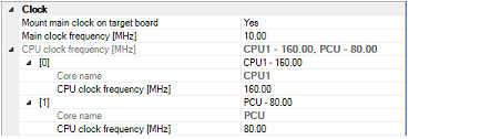
Select whether to mount the main clock circuit on the target board.
Select [No] when you use the on-chip oscillation circuit instead of the main clock circuit.
Select [Yes] when you use the main clock circuit, and specify its frequency in the [Main clock frequency [MHz]] property.
Note that when [No] is selected, the following properties become fixed values.
[LPD mode]: [4pin]
[Set OPJTAG in LPD connection before connecting]: [No]
Specify the main clock frequency (before multiplication).
You can specify the frequency from the drop-down list or by directly entering a frequency value between 0.001 and 999.999 (unit: MHz) (default: [10.00]).
Specify the CPU clock frequency (after multiplication) for each core.
The names of cores incorporated in the selected microcontroller are displayed as subproperties of this property. You can specify the frequency for each core from the drop-down list or by directly entering a frequency value between 0.001 and 999.999 (unit: MHz).
The number of subproperties displayed here and the default value of the CPU clock frequency differ depending on the selected microcontroller.
The CPU clock frequency is used to convert the time stamp information for a trace to an actual time. |
You can configure the connection between E1 and the target board.
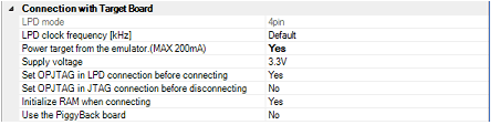
Select LPD communication mode to use.
The selectable pin values differ depending on the selected microcontroller.
Note, however, that this property value cannot be changed when only one communication mode is available.
This property appears only when the [LPD mode] property is set to [1pin].
Select the baud rate for LPD communication (default: [500]).
This property appears only when the [LPD mode] property is set to [4pin].
Select the clock frequency for the LPD communication (default: [Default]).
When [Default] is selected, the default value specific to the microcontroller is used in connection to the target board.
Specify whether power is supplied from E1 to the target system.
Select [Yes] to supply power to the target board (default: [No]).
This property appears only when the [Power target from the emulator (MAX 200mA)] property is set to [Yes].
Select the power voltage supplied to the target board (default: [3.3V]).
Select whether to start up the microcontroller in serial programming mode upon connection to the debug tool and change the option byte settings to select LPD connection.
When [Yes] is selected, the debug tool starts up the microcontroller in serial programming mode upon its connection to CS+. The debug tool then checks the OPJTAG byte and, if LPD is not selected, changes the setting to select LPD. After that, the microcontroller enters debugging mode (default).
When [No] is selected, the debug tool starts up the microcontroller in debugging mode upon its connection to CS+. The debug tool then checks OPJTAG and, if LPD is not selected, shows a message dialog box.
This property can be changed only when the [Set OPJTAG in LPD connection before connecting] property is set to [Yes].
Select whether to change the option byte settings to select JTAG connection before disconnection of the debug tool.
If you wish to change the option byte settings to select JTAG connection before disconnecting the debug tool, select [Yes].
When [No] (the default setting) is selected, the option byte settings are not changed before the debug tool is disconnected. In this case, LPD mode is applicable as the pin mode.
On connection to E1, CS+ changes the option byte settings if LPD is not selected. For this reason, connecting and disconnecting E1 may change the value of the option bytes. |
Select whether to initialize the RAM when connecting to the debug tool.
Select [No] when the RAM is not initialized (default: [Yes]).
When [No] is selected, debugging can be performed when an ECC error occurs because the RAM is not initialized.
When [No] is selected, an ECC error may also occur during access to the RAM from the Memory panel, Watch panel, Local Variables panel, etc. |
This property only appears when the selected microcontroller requires it.
Select whether to use the PiggyBack board.
Select [Yes] to use the PiggyBack board (default: [No]).
You can configure the flash memory rewriting.
The properties in this category may vary with the selected microcontroller. |
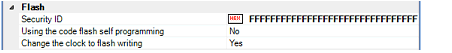
This property appears only when the selected microcontroller supports the ROM security function for flash memory.
Specify the ID code when reading the code from the internal ROM or internal flash memory.
Directly enter 32 digits hexadecimal number (16 bytes) (default: [FFFFFFFFFFFFFFFFFFFFFFFFFFFFFFFF]).
Select whether to rewrite the code flash by using the flash self library of the flash self programming function.
Select [Yes] to rewrite the code flash (default: [No]).
Note that if [Yes] is selected in this property, the code flash will not be cashed.
Select whether to increase the clock speed temporarily for writing to the flash memory by the debugger operation.
Select [Yes] to overclock for writing to the flash memory so that the performance of flash rewrite is improved (default).
When [No] is selected, a flash rewrite is performed using the clock speed set by the user.
Selecting [Yes] may affect the peripheral system that is operating during a break because not only the CPU clock frequency but also the peripheral clock frequency changes. |

Specify the first address of the working RAM area used by the debugger.
Specify the address as a 4-byte unit; if the input value is not a 4-byte unit, it is automatically adjusted.
The firmware of the debugger uses the range from the address where the working RAM is specified to start to the address corresponding to the size indicated in the [Work RAM size [Kbytes]] property.
Since the contents of memory are saved and restored, this area can be used by the user program. However, the area allocated as the working RAM cannot be used in the following ways. |
Display the size of the working RAM area used by the debugger.