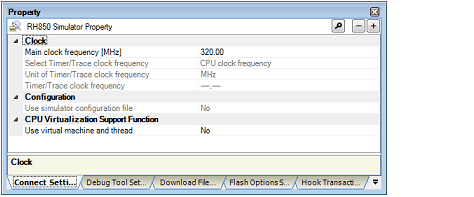
Configure the operating environment on the Property panel below when using Simulator.

Follow the steps below by selecting the corresponding tab on the Property panel.
[Hook Transaction Settings] tab
The simulator is used to simulate instructions of the CPU core assuming that each CPU core type of target MCUs has the number of MPU areas and does or does not have an instruction cache as listed below.
The following notes are also applicable.
The CPU clock operates on the frequency set up with the [Main clock frequency [MHz]] property on the [Connect Settings] tab.
Since the access latency for various memories and peripheral modules is not considered, the execution time (count of cycles) is different from the target device.
Therefore, the following results of the simulator are different from the target device.
[Pipeline] area in the Trace panel |
[Timer] area in the Trace panel |
Trace result when selecting [All core] in the [Trace target] property on the [Debug Tool Settings] tab (Timing between PEs) |
The above sets of information are used as dynamic analysis information for the analysis tools but will differ from results for the actual target devices.
The simulator doesn’t support simulation of peripheral functions.
The following Python functions can be used to generate pseudo interrupts.
See "CS+ Python Console" for detail.
The simulator supports the following types of memory.
Note that with the simulator, however, areas that require special procedures for access according to the specifications of the devices are accessible without following the procedures.
[RH850G3M, RH850G3K, RH850G3MH, RH850G3KH]
External Memory/APB/Data Flash/PBUS/HBUS/Local RAM/Global RAM/AXI/Retention RAM/CPU Peripheral/Code Flash/Video RAM/SDRAM
Note that access to Retention RAM, Video RAM, and SDRAM is handled in the same way as access to Global RAM. |
External Memory/APB/Data Flash/PBUS/HBUS/Local RAM/Cluster RAM/Retention RAM/IBUS/CPU Peripheral/Code Flash/Security Setting Area/Configuration Setting Area/Block Protection Area/Extended Data Area/GTM RAM/Erase Counter/Switch Area/Tag Area/DFP RAM/DFP Peripheral
Access to the Security Setting Area, Configuration Setting Area, Block Protection Area, Extended Data Area, GTM RAM, Erase Counter, Switch Area, Tag Area, DFP RAM and DFP Peripheral is handled in the same way as access to the External Memory. |
System registers that depend on the hardware specifications of the given product, such as the control function registers for the LSU and data buffer and the hardware function registers are not supported.
The simulator doesn’t support the option bytes.
Since the timing of instruction fetching differs between the target device and the simulator, the instruction cache or the number of rounds of access will differ from that on the actual device. |
Even if the target device requires appropriate synchronization processing such as dummy reading or SYNCI instructions, the simulator may operate without such processing. |
Although the cache hit rate (the rate of the number of hits to the number of rounds of cache access) is displayed on the [Cache rate] tab in the Output panel, the rate may differ from that on the target device. |
The error-correcting code (ECC), LRU operation, and information on cache errors in the instruction cache are not supported. |
For FPU instructions and FXU instructions (only for the RH850G4MH), the results of operations will differ between the target device and the simulator. |
[RH850G3K] |
[RH850G4MH] |
Some RH850 MCUs have specific option bytes for selecting the boot mode for the CPUs and IO registers for selecting which CPUs should be booted up when the MCU is reset. The simulator, on the other hand, does not support such facilities and all CPUs are booted up when the MCU is reset. |
The use of SoftFloat technology by this software is under the License for Berkeley SoftFloat Release 3e.
Copyrights of other software components are owned by Renesas Electronics Corporation.